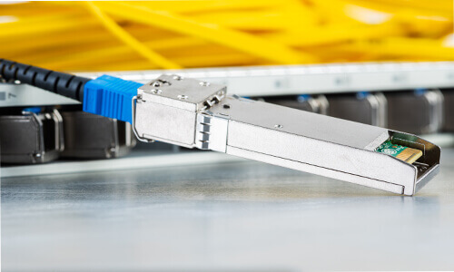
SFP transceiver all-in-one transceiver because of its miniaturization, easy hot plug and play, support for SFF8472 standard, analog reading convenience (IIC reading), and high detection accuracy (+/-2dBm or less) and gradually become the mainstream of the use of the following SFP optical module as an example, to introduce its internal composition and the related principle of operation.

1. Internal Structure of SFP Optical Module
As can be seen in Figure 1, the main part of the optical module is composed of an optical transmitter component, a laser driver, an optical receiver component (the optical receiver part of the L16.2 optical module uses an APD receiver, which also requires a booster circuit), a limiting amplifier and a controller. Driver chips and limiting amplifiers generally support multiple rates from 155Mb/s to 2.67Gb/s. Different rates, different transmission distances of optical modules have a lot of just the front-end optical components of the difference, high speed rate SFP optical module BOM cost of 90% are concentrated in the optical components. From the above chart can also be seen, in order to ensure that the order of power-up, the SFP optical module of the gold finger part of the length is not the same, the longest is the signal ground, followed by the power supply, the shortest is the signal, so that in the plugging and unplugging to ensure that the order of ground, power, signal.
2. TOSA(Transmiter Optical Sub-Assembly)
Commonly used light-emitting components by two categories, one is the use of light-emitting diode LED package TOSA, a class of semiconductor laser diode LD package TOSA. The former spectral line broadening, coupling efficiency is low (although the LED can emit a few milliwatts of optical power, but the directionality of the poor, can be coupled to the fiber optic transmission for the part of the part accounts for only 1-2%), but the price is low, long service life is still a small number of applications in the case of low-speed short distance, the wavelength is generally 1300 nm. Low price, long service life, in the case of low-speed short distance or a small number of applications, commonly used in 100 Gigabit Ethernet multimode fiber in short-distance data transmission, the wavelength is generally 1300 nm. we come into contact with the optical module are generally used in the laser diode.
3. Types of lasers
A. VCSEL lasers
850nm wavelength, used for gigabit tthernet multimode fiber short-haul transmission, gigabit ethernet switches use a large number of optical modules of this type, transmission optical boards will not be used.
B. FP and DFB lasers

The difference between the two lies in the different characteristics of the output light, FP laser is a multi-longitudinal mode laser MLM, can produce light containing a number of discrete wavelengths, in addition to the center wavelength of the primary mode, other wavelengths of the secondary mode also has a high amplitude, and the primary and secondary modes are in the dynamic competition, but the bandwidth range is very narrow.DFB laser is a single-longitudinal mode laser SLM, the main mode optical power accounted for more than 99% of the total power. The primary mode accounts for more than 99% of the total power, and the other small amount of secondary mode is negligible.
For these two different types of laser optical modules, the method of testing their spectral widths with a spectrometer is different.
For FP laser optical modules, the spectral width on the transmitter side is tested for RMS spectral width.
For DFB lasers, the spectral width of the transmitter side is tested at -20dB, and the side-mode rejection ratio is required to be tested.
Currently in the optical modules we use, 155M, 622M module emission wavelength of 1310nm, using the FP laser, 1550nm wavelength is used in the DFB laser. 2.5G in addition to the 2Km that is, the I-16 use FP lasers, the other are used in the DFB laser.

The resonant cavity of the laser diode has two reflective mirrors, which are translucent. Their role on the one hand constitutes a resonant cavity to ensure that the photons in which the reciprocating motion in order to elicit new photons, on the other hand, a significant portion of the photons from the mirrors to transmit out that is, luminescence. The light transmitted out of the front mirror is called the main light, through the coupling with the optical fiber to send the optical fiber into a useful transmission. The light emitted from the rear mirror is called the secondary light or backlight, and TOSA converts this backlight into a backlight current, which can be used to monitor the magnitude of the luminous power of the light source device.

The above figure shows the variation of input current and output optical power of the laser in case of temperature increase.
When the optical gain in the laser cavity exceeds the loss in the reflecting surface at the cavity end, the laser excites a coherent optical signal, and the current in the laser at threshold is called the threshold current (Ith).
As the temperature rises the optical gain in the laser cavity decreases, due to the decrease in the optical gain within the cavity, the laser requires a larger injection current to obtain a coherent optical output, and as a result the threshold current of the laser rises.
As can be seen from the above figure, the increase in threshold current results in a decrease in output optical power, and the driver must output a larger bias current if the optical power is to remain constant. In order to compensate for the laser threshold changes, the need to use the “automatic power control (APC)” circuit, the APC circuit monitors the laser backlight current, by adjusting the laser bias current to maintain the stability of the backlight current.
Generally, the proportionality between the backlight current and the average optical power is linear, so by keeping the backlight current stable, the average optical power of the laser is kept constant.
As shown in the above figure, with the increase of temperature, the slope of the characteristic curve of the laser input current and output optical power will become smaller, which means that the efficiency of the laser photoelectric conversion is reduced.
We know that the extinction ratio Er = 10 × lg [P1 / P0] (dB), where P1, P0 represent the digital logic signal “1” and “0” when the laser output optical power, P1-P0 represent the amplitude of the optical signal after modulation.
Assuming that the output optical power remains unchanged, a decrease in the conversion slope will cause a decrease in the extinction ratio of the output optical signal, which will be reflected in the eye diagram, and the opening of the eye diagram will become smaller.
For the optical module, in the process of temperature change, in addition to maintaining the stability of the output optical power, but also to maintain the stability of the extinction ratio. To keep the extinction ratio stable is to increase the modulation current, the most common practice is to look up the meter method, using the digital adjustable potentiometer (resistor) inside the controller to maintain the extinction ratio.
Built into the digital potentiometer is a temperature-controlled resistance value meter, with the resistance value stored in non-volatile memory as a function of temperature over a temperature range from -45°C to +95°C in steps of 2°C. Using the temperature sensor integrated within the chip, the resistance value of this resistor can be automatically adjusted as the temperature changes.
Digital potentiometer is set to reduce the resistance value as the temperature rises, connected to the driver’s “modulation current setting terminal”, in the process of temperature rise, the controller according to the measured temperature value of the table, and constantly reduce the resistance value of the potentiometer, so that the modulation current increases, so that the extinction ratio of the changes in the light will be compensated.
To maintain the extinction ratio, there is another method is the K factor compensation method, the laser driver to join the “K-factor” compensation feature, it is in the laser bias current increases at the same time, proportionally increasing the modulation current.
The process is as follows: in order to maintain a stable average optical power, bias current is controlled by the APC circuit, with the bias current increases, the circuit extracts a part of the bias current to regulate the modulation current.
In this way, the total modulation current is equal to the original modulation current plus bias current multiplied by a factor K. This K factor can be set by the driver chip external resistor, because the modulation current can increase with the bias current increases, so when the laser temperature changes or laser aging, the extinction ratio can be compensated.
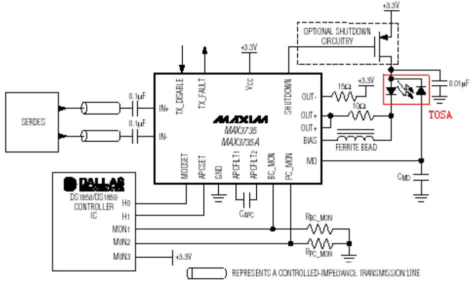
The figure shows a typical control circuit for the look-up table method. In the controller, H0 and H1 are two digital potentiometers that come with the controller, H0 is used to control the modulation current and H1 is used to control the bias current.
The APC function is integrated inside the driver, but its compensation ability is often limited in such a wide range as -40 to 85 degrees, so H1 is used to achieve coarse adjustment, and the APC inside the driver achieves more accurate auto tuning. These two digital potentiometers are using the look-up table method.
Specific resistance value is based on the optical module manufacturers to figure out the characteristics of the TOSA set, often for different manufacturers or different batches of TOSA, have to re-correct the resistance value.
MON1 is used to detect the value of the bias current, MON2 is used to detect the output optical power, and MON3 is generally used for the detection of the received optical power.
These measured values can be obtained through the IIC bus to read the corresponding registers, easy to use, high precision, the vast majority of manufacturers to ensure that the accuracy of control within 2dBm, which can effectively avoid some of the current single-board analog detection is not allowed to this problem.
From the figure can also be seen, the working principle of the optical module in addition to maintaining a stable optical power and extinction ratio, is to do a good job of the driver to the laser between the RC matching (the above figure is not drawn, after the serial 10 ohm resistor, generally need to add RC circuits to the ground), the optical module of the optical interface indicators of the good and bad are determined by these RC.
4. ROSA(Receiver Optical Sub-Assembly)
ROSA inside the package of photodetection diodes and mutual resistance amplifier TIA photodetection diodes, PIN tubes and APD avalanche diodes of two types.
APD photodiode has a multiplier effect, can make the same size of light under the action of the PIN photodiode than dozens of times or even hundreds of times the photocurrent, equivalent to play a role in a kind of optical amplification (in fact, not a real optical amplification), so can greatly improve the sensitivity of the optical receiver (more than the PIN optical receiver to improve the more than about 10dB).
However, the multiplier effect of APD will make the noise coupled into the ROSA will also be amplified at the same time, affecting the sensitivity of the receiver, so the use of APD as a receiver for the optical module needs to deal with filtering and other issues.
For receivers, the optical power is higher than the overload point or lower than the sensitivity, both of which may result in BER or LOF.
The overload point of PIN tube is -3dBm (generally can reach 0dBm), APD is -9dBm (generally can reach -5dBm), for APD receiver, because of its low overload power, if the received power is too high, it may cause breakdown damage.
In the optical modules we use, except for L16.1 and L16.2 optical modules that use APD receivers, the rest of them use PIN tube receivers.

On the receive side of the Transceiver, for the 2.5G output, some vendors have CML output and some have LVPECL output, so you need to pay attention to their Datasheets.
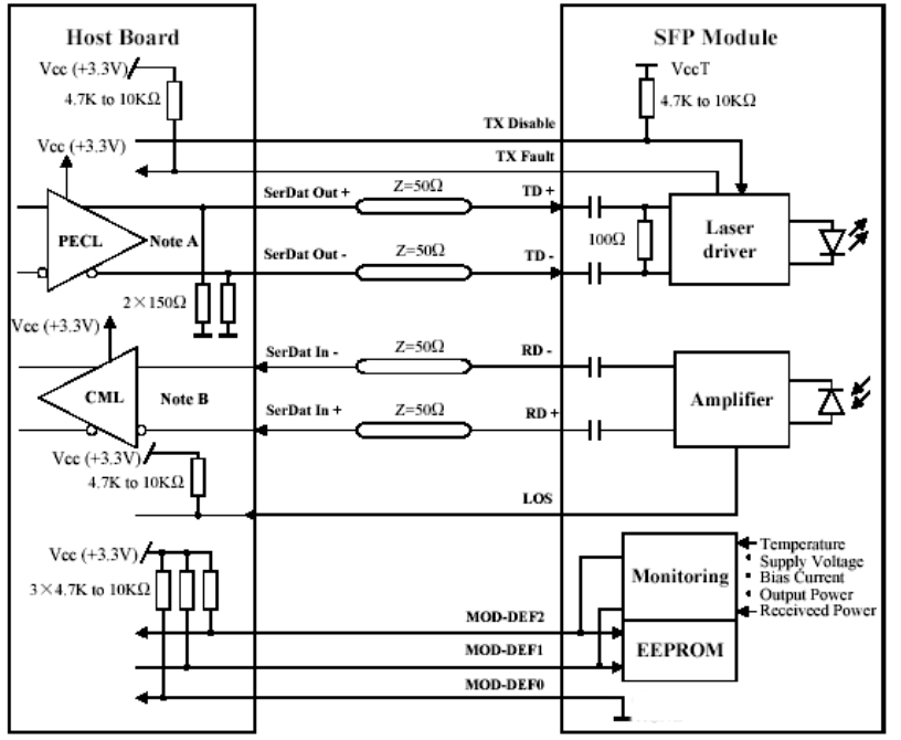
1) Most manufacturers of SFP modules use internal AC coupling, and the module also has a good internal pull-up and pull-down matching, so there is no need to add matching on this side near the optical module.
2) For MOD_DEF0 (optical module in place), MOD_DEF1 (IIC Clock), MOD_DEF0 (IIC Data), LOS (and SFF definition of the opposite, high for no light input, low for normal. SFF is Signal Detect, SD high for light signals, low for no light signals), Tx_Fault (Transmit Fail) all must be pulled up on the user side.
3) When the SFP detects an abnormal condition that triggers protection shutdown, Tx_Fault becomes high and there is no light output, it must be reset with the Tx_Disable signal.